PCB design
From a two-layer proof of concept to a 16-layer high-speed board, we design PCBs that come up on the first spin and go straight to manufacturing: controlled impedance, length-matched buses, clean power and a complete production package.
Boards ready for AI
Edge AI needs more than a fast chip: room for cameras and microphones, clean power for the processor or NPU, and a thermal budget that holds up inside an enclosure.
See AI integration- Edge processor and NPU layouts
- Camera and MIPI interfaces
- Power and thermal design
What we do
Schematics and layouts from 2 to 16 layers, checked for signal integrity and ready for the fab.
Multi-layer boards
Stack-ups from 2 to 16 layers with controlled impedance, differential pairs and dedicated power and ground planes.
- 2 to 16 layers
- HDI
- Blind and buried vias
High-speed digital
DDR, PCIe and NVMe, USB 3, MIPI DSI and Gigabit Ethernet routed with length matching, pair tuning and crosstalk control.
- DDR4 and DDR5
- PCIe and NVMe
- MIPI DSI
- SI analysis
RF and antennas
Sub-GHz, 2.4 GHz and 5 GHz layouts with ground stitching, matching networks and coplanar waveguides.
- 50 Ω lines
- Wi-Fi and BLE
- LoRa
Power electronics
Switch-mode supplies, DC-DC converters, battery management and motor drives designed for efficiency, low EMI and heat.
- SMPS
- BMS
- Motor drives
- Protection
Industrial and harsh environments
IPC-2221 Class 3 practice, isolated I/O, surge and reverse-polarity protection, CAN and RS-485, and wide temperature ranges.
- Isolation
- Surge protection
- CAN and RS-485
DFM and design review
Manufacturing checks against your fab's limits, plus reviews of existing designs using our in-house netlist checker and ODB++ analysis.
- DFM
- Netlist checks
- ODB++
Design capabilities
The standards and tools behind every release.
- Layer count
- 2 to 16 layers
- Minimum trace and space
- 3 mil / 3 mil
- Minimum drill
- 0.2 mm (laser via)
- Board materials
- FR4, Rogers, polyimide
- Maximum board size
- 600 × 500 mm
- Component pitch
- Down to 0.3 mm BGA
- Signal speed
- Up to 10 Gbps SerDes
- Impedance control
- ±10%
- Via types
- Through, blind, buried, micro
- Surface finish
- ENIG, HASL, OSP, immersion silver
- Copper weight
- 0.5 to 6 oz/ft²
- Simulation
- SPICE, signal and power integrity
Final limits depend on the fabrication house you choose; we check them before layout starts.
How a project runs
- 01
Requirements and stack-up
Signal types, fab capabilities and cost targets set the stack-up and design rules before a single trace is routed.
- Design rules
- Stack-up sheet
- Fab capability review
- 02
Schematic capture and review
Hierarchical schematics with net classes and a parametric BOM, checked against the specification and our netlist rules.
- Schematic PDF
- Netlist
- BOM draft
- ERC report
- 03
Placement
Decoupling, clocks, RF sections and high-current paths placed for electrical performance first.
- Placement review
- Thermal zoning
- EMC pre-check
- 04
Routing and SI
Power planes and critical nets first: pairs length-matched, buses checked with impedance simulation, DRC run throughout.
- Length matching
- Impedance simulation
- Clean DRC
- 05
DFM and final review
A full manufacturing audit: clearances, silkscreen, copper islands, test points and testability.
- DFM report
- Testability review
- 06
Production package
Everything a fab and assembly house need, with revision history.
- Gerber X2
- ODB++
- Pick-and-place
- Final BOM
What you receive
Everything is yours at handover, including the source and its history.
Schematic files
Native project files and PDF schematics with full hierarchy.
Gerber X2 and drill
Fabrication files, Excellon drill data and an ODB++ package.
Bill of materials
Manufacturer part numbers, alternates and cost breakdown.
Assembly drawings
Top and bottom views with designators and orientation marks.
Pick-and-place file
XY coordinates for SMT assembly machines.
SI and DFM reports
Signal-integrity results (eye diagrams, crosstalk, S-parameters and impedance) and the full manufacturing audit.
3D STEP model
For mechanical fit checks and enclosure design.
Revision history
Version-controlled design with a change log.
Tools we use
Primary EDA
Altium Designer
Complex multi-layer boards, simulation and output generation.
Open source
KiCad
Open-hardware and cost-sensitive projects, with Python automation.
Enterprise
Cadence Allegro and OrCAD
Dense, high-speed designs and OrCAD-format deliverables.
Simulation
LTspice
Power supplies, filters and pre-layout checks.
In-house
NetGuard
Our netlist checker that catches pin-role mistakes ERC misses.
Related work
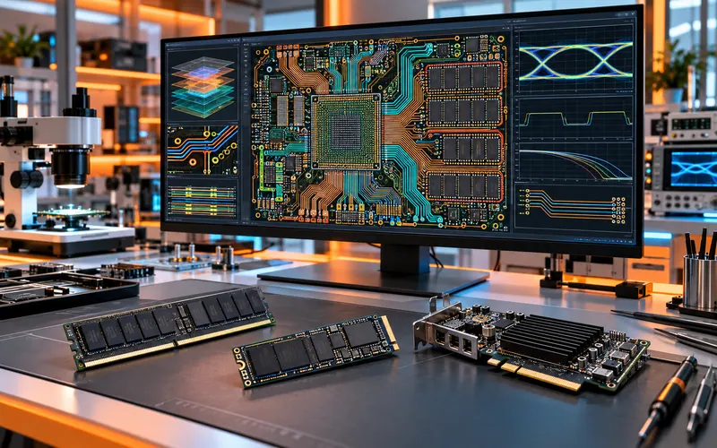
Complex high-speed boards, from our own RAM to AI cards
Our own RAM, SATA III, NVMe M.2 and PCIe SSDs, an AI card and a high-speed single-board computer, on PCBs from 4 to 12 layers, with signal-integrity, eye-diagram and crosstalk reports.
Read the case study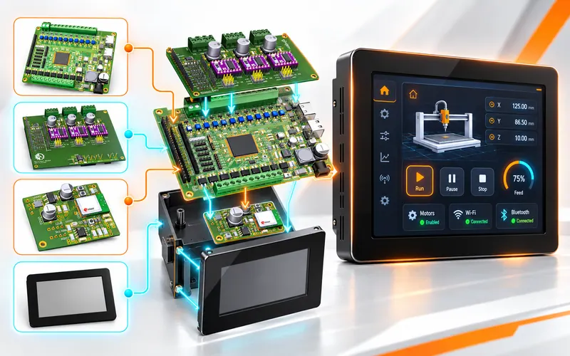 AI inside
An industrial controller you program by describing it
Our own STM32-based controller and the Shree-Mazu Workbench, which generates and flashes its firmware from a canvas or a plain-English request.
Read the case study
The Diamond Planner machine, designed end to end
A machine that scans a rough diamond in 3D and plans the most valuable stones inside it, using our own gravity-based optimization. We designed all of it: the mechanics, the 6-axis controller board and the software.
Read the case studyReady to make your machine smarter?
Tell us about the machine you run or the product you imagine. We reply within 24 hours on working days. We sign an NDA before you share details.