Complex high-speed boards, from our own RAM to AI cards
Our own RAM, SATA III, NVMe M.2 and PCIe SSDs, an AI card and a high-speed single-board computer, on PCBs from 4 to 12 layers, with signal-integrity, eye-diagram and crosstalk reports.
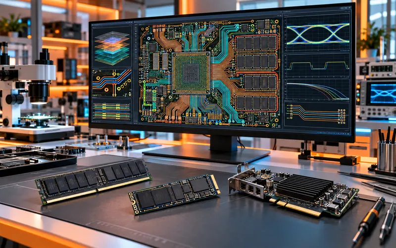
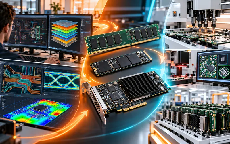
Six kinds of high-speed board, designed in-house
Memory, storage, AI and computing: boards where the layout decides whether the product works. Each was designed by our team, from the stack-up to the production files.
- kinds of high-speed board
- 6
- PCB layers
- 4–12
RAM module
Our own memory module: dense DRAM routing with byte lanes matched to their strobes.
SATA III SSD
A 6 Gb/s SATA link, flash memory and controller on one compact board.
NVMe M.2 SSD
PCIe lanes and flash packed into the narrow M.2 form factor.
PCIe SSD
A storage card that plugs straight into a PCIe slot.
AI card
A board built around an AI processor, with high-speed links to its host.
High-speed single-board computer
A complete computer on one board: processor, memory and high-speed interfaces.
The challenge
Memory, storage and AI boards move data at gigabits per second across a few centimetres of copper. At those speeds every trace behaves as a transmission line: a wrong stack-up, an unmatched pair, a long via stub or a broken return path closes the eye, and a board that works on the bench fails in the field. The same boards pack fine-pitch BGAs, dense memory and many power rails into very little space.
What we built
So far we have designed our own RAM module, a SATA III SSD, an NVMe M.2 SSD, a PCIe SSD, an AI card and a high-speed single-board computer, on PCBs from 4 to 12 layers. Each one started from a stack-up agreed with the fabricator and routing rules taken from the interface specifications, was routed to controlled impedance with matched lengths, and was checked in simulation before release. The signal-integrity report, with eye diagrams and crosstalk analysis, goes out with the manufacturing files.
Engineering highlights
- Controlled-impedance stack-ups from 4 to 12 layers, agreed with the fabricator before routing starts
- Differential pairs for PCIe, NVMe and SATA III matched in length and kept on solid reference planes
- DDR memory routed with byte lanes matched to their strobes and clean address and command timing
- Fine-pitch BGA fan-out, with via transitions and stubs checked on every high-speed net
- Decoupling and power planes laid out around fast processors, controllers and memory
- Eye-diagram, crosstalk and S-parameter results delivered with the manufacturing files
How we design a high-speed board
- 01
Stack-up and rules
Layer count, materials and trace widths are agreed with the fabricator for each impedance target, and the interface specifications become routing rules.
- Stack-up
- Impedance table
- Routing rules
- 02
Placement and routing
Fine-pitch BGAs fanned out, differential pairs matched, memory lanes tuned, and every high-speed net kept on a solid reference plane.
- Placement review
- Length matching
- 03
Simulation and reports
Eye diagrams, crosstalk, S-parameters and impedance are checked before release; anything short of margin goes back into the layout.
- SI report
- Eye diagrams
- Crosstalk
- 04
Production and bring-up
Fabrication and assembly files with impedance and drill notes, then the first boards are brought up and tested.
- Gerber and ODB++
- Assembly files
- Bring-up
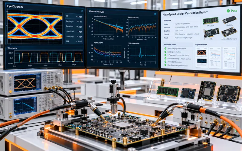
Signal-integrity reports with every high-speed board
The report goes out with the manufacturing files, so you, your customer or a test lab can see the margins before the first board is built.
Signal-integrity check
Every high-speed net checked against its rules: impedance, length matching, spacing and return paths.
Eye diagrams
Eye height, eye width and jitter for each link, compared with the interface's mask.
Crosstalk (NEXT and FEXT)
Near- and far-end coupling between neighbouring nets, and the spacing that keeps it in budget.
Insertion and return loss
S-parameters (S11, S21, S12 and S22) of each channel, from the chip through vias and connectors.
Impedance profile (TDR)
The impedance along each line, showing every discontinuity at vias, pads and connectors.
Margin, jitter and BER
How much margin each link has left, with an estimate of jitter and bit error rate.
More work
All work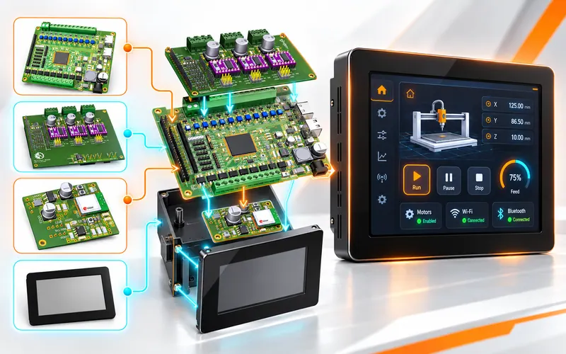 AI inside
An industrial controller you program by describing it
Our own STM32-based controller and the Shree-Mazu Workbench, which generates and flashes its firmware from a canvas or a plain-English request.
Read the case study
The Diamond Planner machine, designed end to end
A machine that scans a rough diamond in 3D and plans the most valuable stones inside it, using our own gravity-based optimization. We designed all of it: the mechanics, the 6-axis controller board and the software.
Read the case study AI inside
Shree-Mazu Smart Home: design in VR, live in reality
It creates a virtual world with your own home and your own 3D character. Your family sets up lights, scenes and devices there like playing a game, and our AI transfers the result to your real home.
Read the case studyReady to make your machine smarter?
Tell us about the machine you run or the product you imagine. We reply within 24 hours on working days. We sign an NDA before you share details.